JEOL
76+ years of electron beam optics development applied to additive manufacturing
www.jeolusa.com
From the Manufacturer
The Only Company Applying 76+ Years of Electron Beam Optics Development into Additive Manufacturing Solutions
Established in Tokyo in 1949, JEOL is a world leader in analytical instrumentation and electron optical equipment for high-end scientific and industrial research and development. Core product groups include SEM and TEM electron microscopes and e-beam lithography systems, as well as MS, NMR, and ESR analytical instruments.
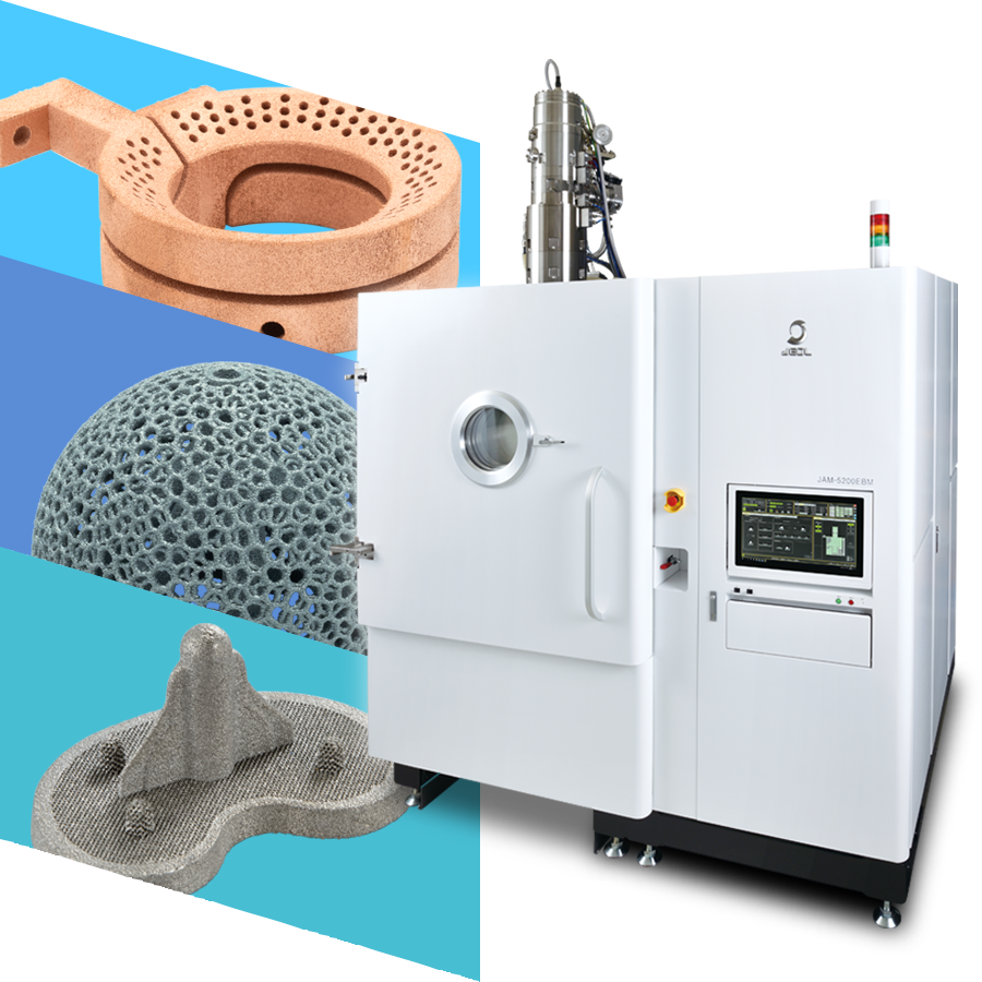
JEOL's JAM-5200EBM distinguishes itself through its cutting-edge Electron Beam Powder Bed Fusion (EB-PBF) technology. Equipped with a robust 6kW electron beam, the beam operates at scanning speeds a thousand times faster than conventional lasers used in similar technologies. JEOL's technology also eliminates multiple post-processing steps that are traditionally necessary in metal 3D printing, such as stress relief heat treatments and wire electrical discharge machining (EDM).
JEOL has also introduced Backscattered Electron Imaging (BSE) per layer, a capability born from our Scanning Electron Microscopy (SEM) division. This enables 100X+ resolution of the melted layer vs camera-based imaging as direct atomic interaction reveals all defects, including pores and cracks.
With EB-PBF, fully dense Tungsten and refractory metal parts can be printed effectively due to the high power electron beam and prevention of oxidation from its vacuum environment. For Tungsten, the powder bed temperature is maintained at 1600°C prior to melting, well above the Ductile to Brittle Transition Temperature (DBTT), preventing crack formation during cooling. This new refractory metal printing capability enables industries such as nuclear fusion, hypersonics and defense to produce optimized parts with DfAM features.
Visit JEOL WebsiteJAM-5200EBM — Electron Beam Powder Bed Fusion (PBF-EB/M) Specifications
| Machine | Build Volume | Process Monitoring | Print Materials | Beam Power / Speed |
|---|---|---|---|---|
| JAM-5200EBM | 250mm diameter × 400mm height | Backscattered Electron Imaging, Camera Imaging, IR Camera | Ti6Al4V, Tungsten, Nickel Alloy 718, Copper, and more | 6000W / 1000 m/s |
TCT Buyer Guidance
Questions for your JEOL EB-PBF evaluation
Are you working with reactive or refractory metals? EB-PBF's vacuum environment and high preheat temperatures make it a strong candidate for titanium, tungsten, and nickel superalloys where oxidation and cracking are critical concerns.
What surface finish does your application require? EB-PBF typically produces rougher as-built surfaces than laser PBF (Ra 20--35 µm vs 5--15 µm). If your parts require fine surface finish, factor in additional post-processing but weigh this against the elimination of stress relief and support removal.
What is your quality assurance framework? EB-PBF systems with in-situ monitoring (BSE imaging, IR cameras) can provide layer-by-layer inspection data that feeds directly into qualification workflows. This can be a significant advantage for aerospace and medical applications.